Researchers are designing ways to improve the mechanical strength of materials for a variety of applications, especially electronics, writes Rajashree Nori
The pleasure of owning the latest smartphone is undescribable. The myriad ways in which it lets you be more productive and share precious moments is baffling. But the pain hits you when your smartphone goes blank after you accidentally drop it on the floor. Similar is the ordeal with your ultra-smart laptop or tablet. Admit it! We all have had embarrassing incidents with our electronic devices.
Clearly, packing in more features into state-of-the-art gadgets is no longer enough. As technology becomes more pervasive and integral to our lives, the call for them to be more robust becomes louder. So, how do we make our electronic gadgets stronger without sacrificing their light weight and handy size? Praveen Kumar and his team from the Indian Institute of Science (IISc), Bengaluru have discovered that one of the answers lies in using electricity itself.
Work in progress
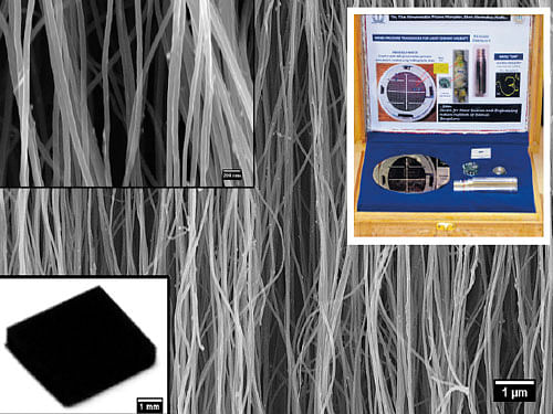
His team is developing ways to increase the strength of carbon nanotube (CNT) foam, to replace the standard polymer foam used inside electronic gadgets for shock absorption. The foam is a dense mesh of carbon nanotubes routinely studied for mechanical applications. Their recent experiments show that applying a voltage of 1V during a fall can increase the shock absorption capacity of CNT foam by 3 times. This new finding can be implemented in the near future because “such a small voltage is easily available in a phone or laptop battery,” says Praveen.
In the Thermo-Electro-Mechanical Behaviour Laboratory at IISc, Praveen and his team design ways to improve mechanical strength of materials for a variety of applications, especially electronics. They identify, investigate and engineer solutions for all possible causes for failure in futuristic devices — such as mechanical shock, high currents and excessive heat.
But why are these factors so troublesome in electronics today? The main reason lies in miniaturisation. To get smaller, multifunctional gadgets, engineers pack in more transistors in an electronic chip and more chips in a circuit board. This leads to higher current densities confined in a small space, in turn leading to more heat generation.
Laptops today can heat up to 60 degrees Celsius with continuous usage. This temperature is high enough to cause structural weakness in the environmentally-benign lead-free solders used in circuits today. Additionally, high current densities weaken the bond between the tin-based solders and copper wires, further reducing their life.
Beyond the basics
Connection between electricity and mechanical failure is not new. Electromigration, i.e., flow of metal due to high electric currents, used to be notorious in breaking aluminium interconnect wires within integrated circuits (ICs) over 40 years ago. Aluminium was later replaced with copper, which has a higher melting point and is more robust against electromigration. However, rising heat and current density in devices in last 15 years has led to the resurgence of serious electromigration problems in copper wires as well. Praveen’s group is designing solutions for these problems and also developing new materials that can withstand high currents. What sets them apart is that they have also found a way to benefit from electromigration!
“It was all serendipity,” reminisces Praveen about the experiment where they first observed that they could melt metal and control the direction of its flow using electric field. This gave birth to ‘electro-lithography’ — a new method of creating patterns using only electric field. Conventional lithography needs UV light and masks with precisely drawn outlines to create device patterns on the semiconductor. It is one of the most expensive steps in any semiconductor device fabrication today. In comparison, electro-lithography is inexpensive and simpler to execute. All it needs is a movable electrode tip and metal.
“It is like writing with a quill,” explains Praveen, “if I keep the quill at a spot, the liquid will spread out. Instead, if I move the quill, I can actually write with it.” Using electro-lithography, Praveen and his colleagues have written patterns as small as 40 nm on semiconductors. Their research aims to provide lasting solutions and new techniques that can give us more reliable and economical electronic devices in the future. The group also studies the effect of heat on mechanical stability for other applications — such as aeroplane turbine coatings, solar cells, etc. Bringing together students and experts from material sciences, applied physics, mechanical engineering and electrical engineering, this team is eager to explore all new aspects of mechanical reliability, material behaviour and their close connection to electricity. “After all, some of these things start with a little bit of imagination,” says Praveen.
Deccan Herald is on WhatsApp Channels| Join now for Breaking News & Editor's Picks